
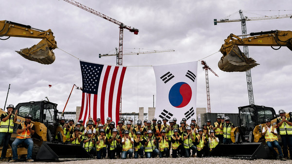
SK Hynix has broken ground on a high‑bandwidth memory (HBM) advanced packaging facility in West Lafayette, Indiana, committing more than $4 billion to build production and research capacity intended to support the United States’ AI semiconductor supply chain. The South Korea–based chipmaker plans to complete a cleanroom by October 2028 and begin U.S. mass production of HBM in the second half of 2029, marking the first time its HBM products will carry a “Made in USA” label after final processing.
The groundbreaking took place on September 27, local time, at Purdue University’s Holloway Gymnasium. Beyond manufacturing lines, SK Hynix will establish an on‑site R&D testbed for advanced packaging, enabling customers, university researchers, and suppliers to co‑develop next‑generation integration techniques and validate prototypes. The company expects the Indiana operation to employ about 1,000 people when production ramps up and estimates roughly 7,000 direct and indirect jobs tied to construction, plant operations, and supplier activity. More than 100 materials, component, and equipment partners are discussing entry into the West Lafayette ecosystem, according to the firm.
The Indiana plant will serve as the back‑end node in SK Hynix’s global HBM chain. Advanced wafers fabricated in South Korea will be shipped to Indiana for assembly, advanced packaging, and testing before delivery to U.S. customers. Advanced packaging—post‑fabrication processes that combine or vertically stack multiple chips—has become central to overcoming scaling limits in traditional miniaturization. HBM, which stacks multiple DRAM dies to dramatically raise bandwidth while improving energy efficiency, is a core component for AI accelerators and data‑center semiconductors.
U.S. officials signaled strong support for the project. Indiana U.S. Senator Todd Young cited the initiative’s potential to create jobs and bolster national and economic security, while Indiana Governor Mike Braun highlighted expected benefits to the state’s technology‑driven growth. SK Hynix CEO Kwak No‑jung framed the U.S. as a hub of AI innovation with key customers and a robust research ecosystem, adding that the Indiana site is intended to become a central HBM supply base for the American market.
SK Hynix also signed a memorandum of understanding with Purdue University to collaborate on next‑generation system integration and advanced packaging research. The company said it aims to broaden industry‑academic partnerships across Midwestern institutions to cultivate semiconductor talent and deepen local R&D capabilities. Separately, SK Group plans to participate as an employer in a job platform operated by the Korea Chamber of Commerce and Industry and the Korean–U.S. Alliance Foundation to provide opportunities for U.S. Forces Korea veterans.
With construction underway, the West Lafayette site is positioned to link SK Hynix’s Korean wafer production to U.S. advanced packaging at scale. If the timeline holds, the facility will bring customer‑proximate HBM output online in 2029, expanding domestic access to a component increasingly vital to AI computing.